- ▪ Instrument
- ▪ PV instrument
- ▪ Instrument for Silicon Material
- ▪ Instrument for CZ&DSS
- ▪ Instrument for Wafer
- ▪ Instrument for Solar Cell
- ▪ Instrument for Module
- ▪ Instrument for PV Station
- ▪ LED instrument
- ▪ Other instrument
- ▪ Consumables
- ▪ Consumables
- ▪ Accessories
- ▪ Software
- ▪ Process software
- ▪ System software
- ▪ Application Software
- ▪ Intrument exchange
- ▪ Overview
- ▪ Exchange flow
- ▪ Exchange notice
- ▪ Exchange Center
- ▪ PV Plant
- ▪ PV Certification
- ▪ TUV
- ▪ UL
- ▪ CE
- ▪ Maintenance Service
- ▪ PV Equipment Upgrades
- ▪ Auxiliary Equipment Maintenance

Products Brief:
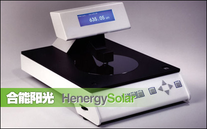
       Manual, non-contact measurement of wafer thickness, TTV and bow. Portable and easy to set-up, the Proforma 300/G measures all wafer materials including Silicon, Gallium-Arsenide, Indium-Phosphide and wafers mounted to sapphire or tape.


Product's Feature:
■Non-contact Measurements.

■Can be used on all wafer materials including: Silicon,Gallium-Arsenide,Indium Phosphide,  Germanium.

■Thickness and TTV values are obtained by placing the wafer between non-contact capacitance probes.

■Thickness and TTV values are indicated on the high resolution LCD display.

■Provides High Performance at Low Cost.

■Menu-driven for Fast, Easy Setup.

■High-resolution LCD Display.

■RS-232 Output Port to PC.

■Parallel Port for Printer.

■Portable and Easy to Set Up

■provides the user precise non-contact measurements at critical points throughout the wafer manufacturing process.

■On-board Microprocessor for Accurate, Repeatable Measurements.

■Teflon Wafer Stage for Easy, Non-abrasive Positioning.


Technique Specification:
■Wafer Sizes: 50mm-300mm.
■Measurement Range: 1mm standard [1.7 mm Extended]

■Thickness Accuracy: +/-0.25um

■Repeatability: 0.050um
■TTV Accuracy: +/-0.05um

■Repeatability: 0.050um
■Bow Range: +/-500um [+/-850um]

■Accuracy :+/-2.0um

■Repeatability: 0.750um
■Material:Silicon,Gallium-Arsenide,Indium Phosphide,Germanium.
■Surfaces: As-cut, Lapped, Etched, Polished, Patterned.
■Flat/Notch: All SEMI Standard Flat(s) or Notch.
■Conductivity: P or N Type.
■Wafer mounting: Bare Wafer, Sapphire/Quartz Base, Tape.
■Continuous and 5-point Measurement.


Application :
■Slicing
>>Saw set-up
    >>>Thickness
    >>>TTV
>>Degradation monitoring
>>>Wire guide re-grooving
>>>Blade replacement
■Lap/etch and polishing
>>Process monitoring
>>Thickness
>>TTV
>>Material removal
>>Bow
>>Warp
>>Flatness
■Backgrind
>>Removal rate
■Final Inspection
>>Lot sampling
>>Final thickness

Typical Customer:
American,Europe and Asia and so on.


